IBM Breaks the 1-Nanometer Barrier With a New 3D Chip Architecture
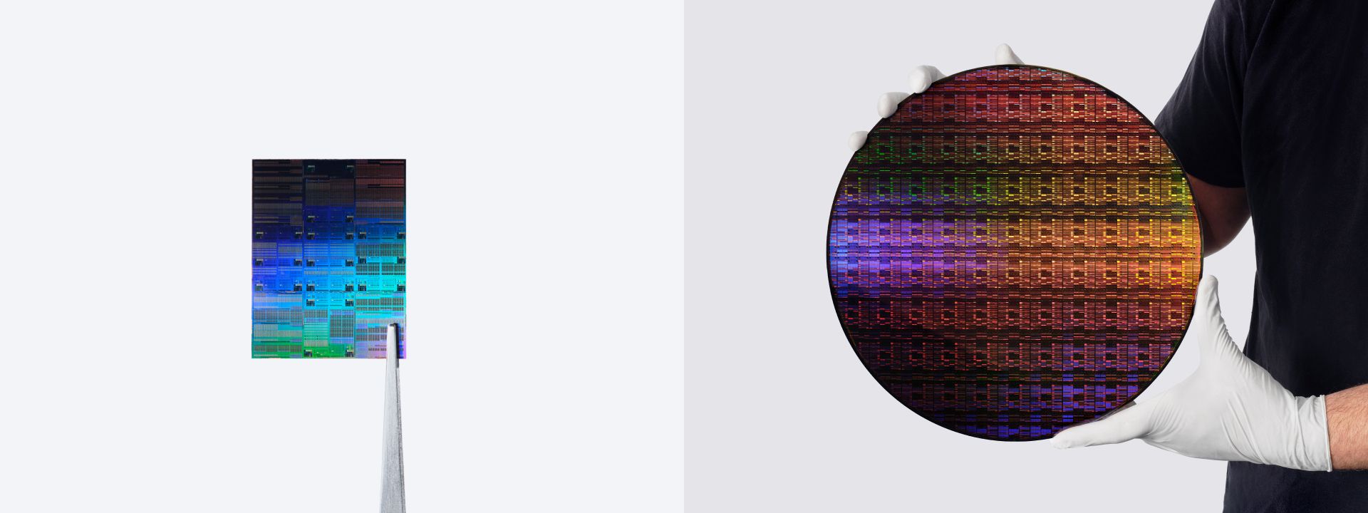
IBM unveiled the world's first sub-1-nanometer chip technology on June 25, 2026, crossing a threshold that many engineers had predicted would end practical semiconductor progress. The breakthrough centers on a new 3D transistor architecture called "nanostack" that stacks transistors vertically rather than shrinking them horizontally, reaching a node of 0.7 nanometers — smaller than a strand of DNA.
A New Way to Build Transistors
The nanostack architecture layers two complete planes of transistors atop each other using a precision bonding technique that keeps individual nanosheets just 15 atoms thick and 9 nanometers apart. Manufacturing requires keeping all processes below 400°C to prevent the bonding layer from melting — a constraint IBM researchers say they have now consistently met at wafer scale. The result is nearly 100 billion transistors packed into a chip the size of a fingernail, roughly double the density of IBM's own 2-nanometer process introduced in 2021.
What the Numbers Actually Mean
Performance numbers suggest the jump is real: IBM says the 0.7nm node delivers up to 50 percent more compute throughput and 70 percent better energy efficiency compared with 2nm chips. SRAM scaling — historically a bottleneck that limits cache density — improved 40 percent, which matters directly for the high-bandwidth memory demands of AI inference workloads.
"This puts another 10, 15 years on the roadmap," said Dan Hutcheson, an analyst at TechInsights, who called the announcement transformational for extending semiconductor timelines. IBM Research Director Jay Gambella described the nanostack as "reinventing how chips are built" rather than simply making existing structures smaller.
What It Means for AI and Energy
As data center operators grapple with the energy cost of training and running large language models, a 70 percent efficiency improvement at the silicon level could reduce the power bill for AI inference at scale by a comparable margin. IBM does not currently manufacture chips in volume — it licenses its process research to foundry partners — but the company says commercialization could begin within five years, placing first products in the market around 2031.
Pressure on Intel, TSMC, and Samsung
For the industry's leading foundries, the announcement raises competitive pressure. TSMC is currently producing at its 2nm N2 node and preparing a 1.4nm A14 process for 2027 or 2028. IBM's jump to 0.7nm does not mean products next year, but it signals that its research pipeline remains ahead of the industry's production frontier by a meaningful margin. IBM stock surged in pre-market trading on June 26 following the announcement.
IBM published full technical details in a research paper released alongside the announcement, covering the CFET architecture, dual-channel engineering approach, and functional CMOS inverter validation at the new node, as reported by MIT Technology Review.
Originally reported by IBM Newsroom. Read the original article for additional details.
View original source