Glass core substrates are replacing organic packaging in next-generation chips
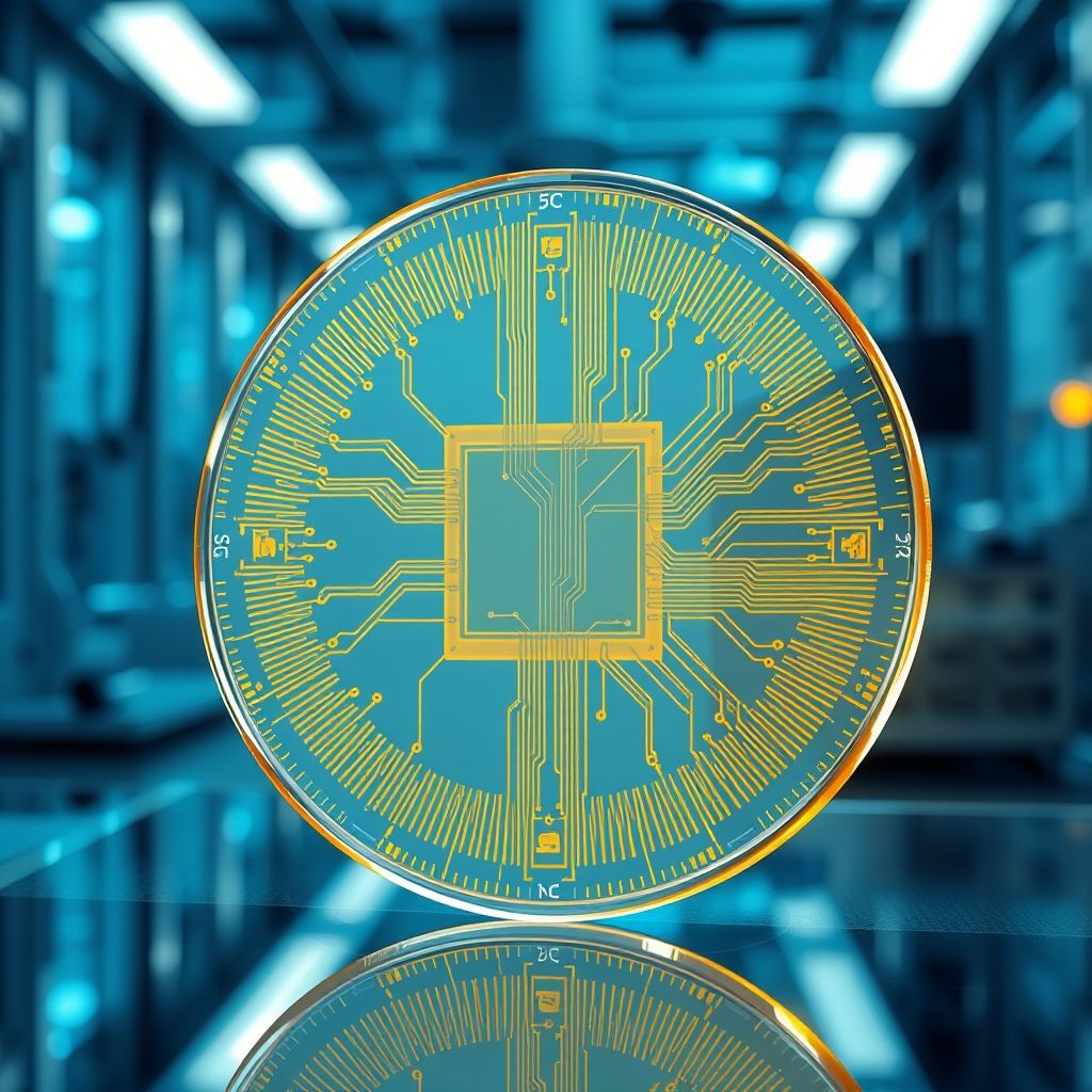
The material holding your CPU's silicon die in place is about to change for the first time in three decades, and the reason is simple: organic substrate packaging has run out of room to keep up with AI accelerators. Intel, Samsung, and SKC's Absolics are now racing toward commercial-scale production of glass core substrates — a shift that will quietly reshape how every advanced chip from GPUs to custom AI ASICs gets built starting in 2026 and 2027.
This is not a cosmetic upgrade. Organic substrates, the resin-based material that has carried chip packaging since the 1990s, physically warp as chips get larger and hotter. At the interconnect densities modern AI accelerators require, that warpage causes misalignment, yield loss, and thermal failures. Glass doesn't have that problem, and the industry has run out of alternatives.
Why Organic Substrates Hit a Wall
Modern AI accelerators — think Nvidia's Blackwell-class GPUs or AMD's MI400 series — pack multiple chiplets onto a single substrate connected by extremely fine interconnects. As package sizes have grown past 100mm to accommodate more compute, organic substrates have struggled with a fundamental physics problem: their coefficient of thermal expansion doesn't match silicon's, so as chips heat and cool during operation, the substrate flexes and warps.
Glass has a thermal expansion coefficient far closer to silicon, and it's dimensionally stable at scale in a way organic materials aren't. Intel's glass substrates demonstrated warpage below 20 micrometers across a 100mm span in early 2026 testing — a tolerance organic packaging cannot reliably hit at that size. That flatness matters because it directly enables denser, finer-pitch interconnects, which is exactly what next-generation chiplet designs need.
Three Companies, Three Different Bets
Intel unveiled its first "thick-core" glass substrate at NEPCON Japan in January 2026, pairing a 10-2-10 layer structure with its existing EMIB multi-chip module technology. Intel has committed to glass substrates since 2023 and is targeting mass production between 2026 and 2030, with capacity plans including a new facility in Odisha, India, built with partner 3DGS, and potential volume manufacturing in Rio Rancho, New Mexico.
Samsung is taking a more vertically integrated route, synchronizing its display division (which already has deep glass manufacturing expertise) with its semiconductor business. Samsung Electro-Mechanics is running a pilot glass substrate line at its Sejong plant, targeting mass production in the second half of 2027, and has reportedly invested in glass substrate specialist JWMT to accelerate its manufacturing capability. Samsung's stated customer targets include Apple, Broadcom, and major cloud providers — a signal it's chasing the same AI-accelerator demand driving Intel's push.
Absolics, a subsidiary of SKC, is arguably ahead on commercial timing. Its Covington, Georgia facility is described as the world's first dedicated "merchant" glass substrate plant — meaning it sells to any customer rather than serving a single parent company's chips. Absolics began shipping mass-production samples to AMD for MI400-series AI accelerators in January 2026 and is targeting full mass production in the second half of 2026, with initial capacity of 12,000 square meters scaling to 72,000 square meters in a second phase.
The Numbers That Matter
Absolics claims its glass substrate technology can cut power consumption by up to 50% and improve signal performance by 30% compared to organic packaging — figures that, if they hold at production scale, would materially change the economics of running large AI clusters where power is already the binding constraint on deployment size. For hyperscalers spending billions on power and cooling infrastructure, a substrate-level efficiency gain compounds across every chip in a data center.
The interconnect density improvement is the other half of the story. Glass substrates support finer redistribution layer pitches than organic materials, which means more signal lines can be packed into the same substrate area. That directly enables the kind of massive chiplet interconnection that next-generation AI accelerators — including Anthropic's newly announced custom inference silicon and Meta's Iris chip — will need as they move beyond monolithic die designs.
What This Means for the Chip Supply Chain
Glass substrate adoption is a slow-motion supply chain shift, not an overnight one. Existing organic substrate suppliers — companies like Ibiden and Unimicron that dominate today's packaging market — face a multi-year transition risk if glass captures the high end of AI accelerator packaging first. Expect the earliest commercial glass substrates to appear in the most expensive, highest-margin chips (flagship AI accelerators, high-end server CPUs) before the technology matures enough to reach consumer devices, similar to how HBM memory rolled out top-down.
For chip designers, glass substrates unlock design freedom that's been constrained by organic packaging's warpage limits for years — larger packages, denser chiplet arrays, and tighter power delivery. For buyers of AI compute, the practical effect will show up as improved performance-per-watt in next-generation accelerators starting in late 2026 and accelerating through 2027, as Absolics, Intel, and Samsung ramp their respective production lines.
The company to watch closest is Absolics, given its earlier production timeline and merchant-market model — it's the first real signal of whether glass substrates can scale beyond a single vendor's captive supply chain into the broader industry.